MOSFET Technical Details
N-Channel vs. P-Channel Symbols
N-Channel and P-Channel MOSFETs have slightly different symbols, with the arrow pointing in or out, depending on the channel type:
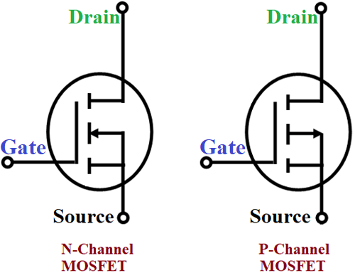
To remember which is which, the following nemonic is useful:
- N-Channel/NPN = "Not Pointing iN."
- P-Channel/PNP = "Points iN Proudly."
MOSFETs Fail Shorted
It's important to select the right MOSFET for the job. Typically, when a MOSFET fails, it fails shorted, meaning that it will no longer switch off and will continuously conduct. This can be extremely dangerous, especially in situations where the MOSFET might control a motor or similar.
Gate Sensitivity
MOSFETs have notoriously sensitive gates to Electro-Static Discharges (ESD). This means that static buildup that hits the Gate can cause the MOSFET to fail. For this reason, many modern MOSFET designs have built in Transient-Voltage Suppression (TVS) diodes built in to the gate.
For example, if you look at the DMN2046UW symbol in its datasheet, it has a built-in TVS gate protection diode.

When sourcing MOSFETs, we generally recommend looking for ones that have gate protection diodes.
You might have also noticed that it has a diode from Source to Drain. It's called a body diode and is just part of how MOSFETs work. They will conduct backwards if installed or wired incorrectly.
Important Switching Specifications
There are a number of important parameters and ratings around the switching characteristics when choosing a MOSFET, the main ones are:
VdssVgs(th)Rds(on)Id(max)
These ratings can be found in the MOSFET's datasheet and can also be used when searching for components on Octopart, Digikey, etc. Though, confusingly, they may not always be named exactly as above.
Maximum Voltage Ratings
Examining the Maximum Ratings table, we can see the maximum voltages that the device can handle:
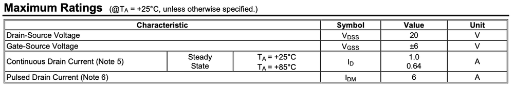
VDSS
The first is the Drain to Source voltage. This is the maximum voltage that the MOSFET can carry between its Drain and Source. This should be greater than the amount of voltage your load needs. For example, if you're expecting to control a 6V motor, the Vdss should be at least 6V, but better if it were a little higher.
It might also be called BVdss which means Drain-Source Breakdown Voltage.
VGS
Maximum Voltage between Gate and Source that the MOSFET can handle. Make sure this is higher than the logic level you're using to control it. For instance this MOSFET can handle a control signal up to 12V.
Switching Behavior/ON Characteristics
Now examining the ON characteristics, it tells us how the device behaves as a switch:
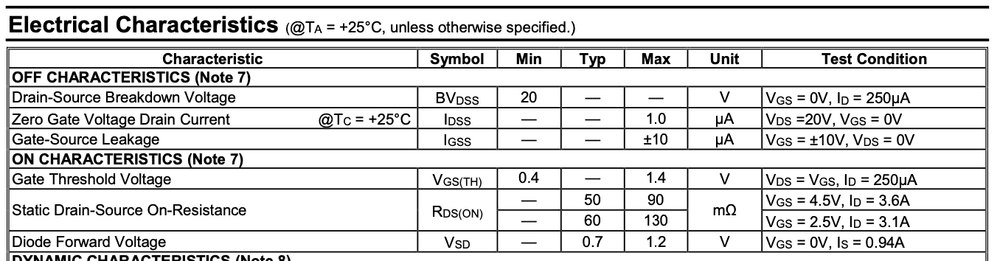
VGS(TH), RDS(ON), & ID
Vgs- Sometimes abbreviated asVTH, theGatetoSourcethreshold voltage is the minimum voltage needed to begin conducting current on the channel betweenGateandSource.Rds(on)- Resistance betweenDrainandSourcewhenON.Id- This is theDraincurrent, or the amount of current that can flow through the MOSFET channel.
These three parameters are used in conjunction to describe how the MOSFET conducts. The Vgs states that at a given voltage to the Gate, the Rds(on) will lower enough that the MOSFET will start letting current flow. Usually in a datasheet, the Rds(on) will be listed with one or more values because how well it conducts is a function of the Vgs. In the image above, we can see that:
- The MOSFET starts to conduct somewhere between
0.4Vand1.4VVgs. Note that this wide range is just an artifact of how MOSFETs work. - At a
Vgsof4.5V, the channel resistance (Rds(on)) is typically around50mΩ, which is50milli-ohms, a very small amount of resistance. And at aVgsof2.5Vit is still very low at60mΩ. - At a
Vgsof4.5V, the channel will typically conduct up to3.6A, and at aVgsof2.5, it'll typically conduct up to3.1A.
This means that this MOSFET is effectively fully on at 2.5V to the Gate. MOSFETs that operate at 5V or less Vgs are referred to as Logic-Level MOSFETs, because you can control them with typical digital logical circuits that nominally run at 5V or 3.3V.
This becomes even more apparent if we look down further in the datasheet and see the graph that tells us what the Rds(on) is at varying Vgs levels:
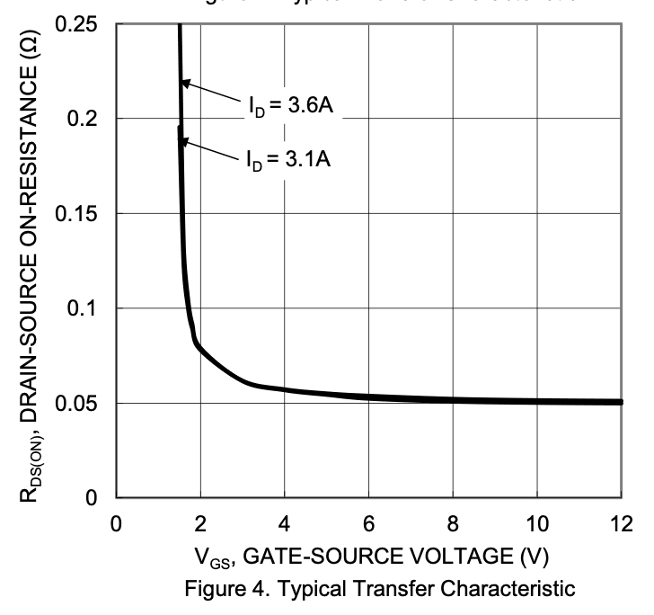
As we can see, the MOSFET actually turns fully on at less than 2V!
Temperature and Power
You'll notice that the specifications are given at Ambient Temperature (Ta) of 25°C/77°F:

This means, that these ratings are good for operations at room temperature, and are the maximum values the device can handle without the need for external cooling such as a heatsink. Many MOSFETs that are meant for switching large loads are designed with a built in plate that can be attached to a copper area on a PCB or a heatsink, and doing so will enable the MOSFET to dissipate more heat and carry a larger load.
Power Rating and Dissipation
MOSFETs are so efficient that for logic control and the small loads typically found in IoT solutions, you rarely have to worry about their power rating.
With that said, if you're switching large loads, it's good to take a look at the power rating fro your MOSFET and calculate whether it can dissipate enough heat without a heat sink or other cooling to not fail.
Calculating the Maximum Power it can dissipate
To calculate the amount of power a MOSFET can safely handle, you'll need the following information from the datasheet:
PD- Maximum it can dissipate without a heatsink.MaxTJ- Maxmimun junction temperature it can withstand (175°C for example)TA- Ambient temperature.RΘJA- Junction to ambient coefficient. Typically specific in°CperWatt.
These specs are usually found in a Thermal Characteristics section:
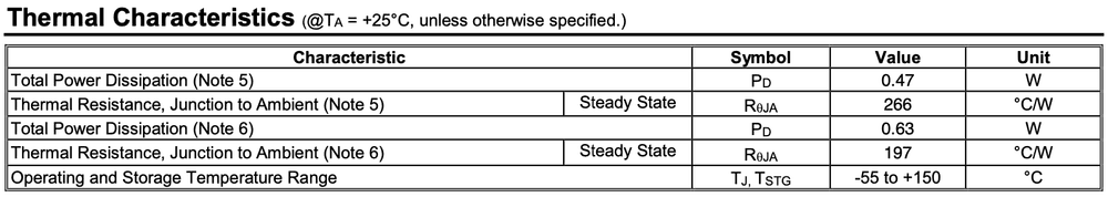
In the case with the table above, two different sets of ratings are given, depending on the PCB composition that it's mounted on. In this case, if it's on a PCB with a heavy copper pour (2oz vs. a typical 1oz thickness) with a large pad, it can dissipate heat much more efficiently:
![]()
Thermal Dissipation Equation
The equation to determine power dissipation is as follows:
PD = (MaxTJ - TA) / RΘJA
So for example, given our MOSFET mounted on just a normal PCB with a standard footprint:
Example:
Pd = (150°C - 25°C) / (266°C/Watt)
Pd = 125/266
Pd = 0.47Watts or 470mW
Therefore, the MOSFET can safely dissipate up to 0.47W without any special considerations.
Calculating Load Power
To calculate how much power your load will use, recall from Part 4 that the power law is:
P = RI^2
In this case, resistance is RDS(ON), and I is the amount of current your load will draw.
So for example, if your RDS(ON) is 50mΩ and your load draws 1A of current:
P = Rds(on) * I^2
Power = 50mΩ * 1A^2
P = 50mΩ * 1A
P = 50mW
In this case, 50mW is considerably less than 470mW, therefore, no heat sink or special considerations are needed.
Packages
The final consideration when choosing MOSFETs is how the component is physically enclosed, also known as the package.
Like most components, MOSFETs come in through-hole (PTH) and surface mount (SMT) designs. However, very few small-signal (logic-level) MOSFETs are actually made in a PTH package.
By far the most common SMT package type that MOSFETs are available in is the Small Outline Transistor (SOT).

SOT23 is probably the most common package you'll find them in, but if you need something smaller but still large enough to assemble by hand, the SOT323 is also a good choice.